Engineers are available to assist.

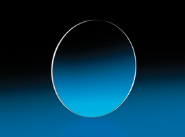
Edmund Optics® (EO), the premier provider of optical components, introduces new TECHSPEC® Fused Silica Wafers. These versatile wafers are thin, circular pieces of UV fused silica designed to be used as test substrates to measure the quality of optical coatings. Fused Silica Wafers are also outstanding for use as dummy components for set-up processes, as well as for semiconductor microlithography or for micro-electronic-optical applications (MEMS).
Ultrasonically cleaned
Edmund Optics’ Fused Silica Wafers Exhibit less than 10Å Surface Roughness with a surface quality of 40-20. Each Fused Silica Wafer has been ultrasonically cleaned and is delivered in contaminant-free packaging to ensure highest quality.
Available in 100 mm, 200 mm and 300 mm diameters
Edmund Optics’ Fused Silica Wafers are available in 100mm, 200mm and 300mm diameter sizes. RoHS compliant, all have thicknesses of 1.00mm and a transmission range of 0.2-2.2μm. Fused Silica Wafers are in-stock and available for immediate delivery for fast turnaround and excellent value.


or view regional numbers
QUOTE TOOL
enter stock numbers to begin
Copyright 2023 | Edmund Optics, Ltd Unit 1, Opus Avenue, Nether Poppleton, York, YO26 6BL, UK
California Consumer Privacy Acts (CCPA): Do Not Sell or Share My Personal Information
California Transparency in Supply Chains Act
This content may include material that has been generated or modified using artificial intelligence (AI).
The FUTURE Depends On Optics®